
EM6520
03/02 REV. D/449
Copyright
2002, EM Microelectronic-Marin SA
1
www.emmicroelectronic.com
MFP version of EM6620
Ultra Low Power Microcontroller 4x8 LCD Driver
Features
� Low Power
- 8 �A active mode, LCD On
- 1.1 �A standby mode, LCD Off
- 0.1 �A sleep mode
@ 3 V, 32 kHz, 25�C
� Large Voltage range, 2 to 5.5 V
� SVLD, default (2.4V)
� EEPROM,
2048
� 16 bits
� RAM, 64 � 4 bits
� 2 clocks per instruction cycle
� 72 basic instructions
� Oscillation
supervisor
� Timer watchdog (2 sec)
� Max. 8 inputs ; port A, port B
� max. 4 outputs ; port B
� LCD 8 segments, 3 or 4 times multiplexed
� Universal 10-bit counter, PWM, event counter
� Prescaler down to 1 Hz (crystal = 32 KHz)
� 1/1000 sec, 12 bit binary coded decimal counter
with hard or software start/stop function
� Frequency output 1Hz, 2048 Hz, 32 KHz, PWM
� 7 internal interrupt sources (BCD counter,
� 2�10-bit counter, 3� prescaler, SVLD)
� 5 external interrupt sources (port A, compare)
Description
The EM6520 is an advanced single chip CMOS 4-
bit microcontroller. It contains EEPROM, RAM,
power on reset, watchdog timer, oscillation
detection circuit, 10 bit up/down counter,
Millisecond counter, prescaler, voltage level detec-
tor (SVLD), compare input, frequency output, LCD
driver and several clock functions. The low voltage
feature and low power consumption make it the
most suitable controller for battery, stand alone and
mobile equipment. The EM6520 is manufactured
using EM Microelectronic's Advanced Low Power
(ALP) CMOS Process.
Typical Applications
� Timing
device
� Medical
applications
� Domestic
appliance
� Timer / sports timing devices
� Safety and security devices
� Automotive controls with display
� Measurement
equipment
� Interactive system with display
� Bicycle
computers
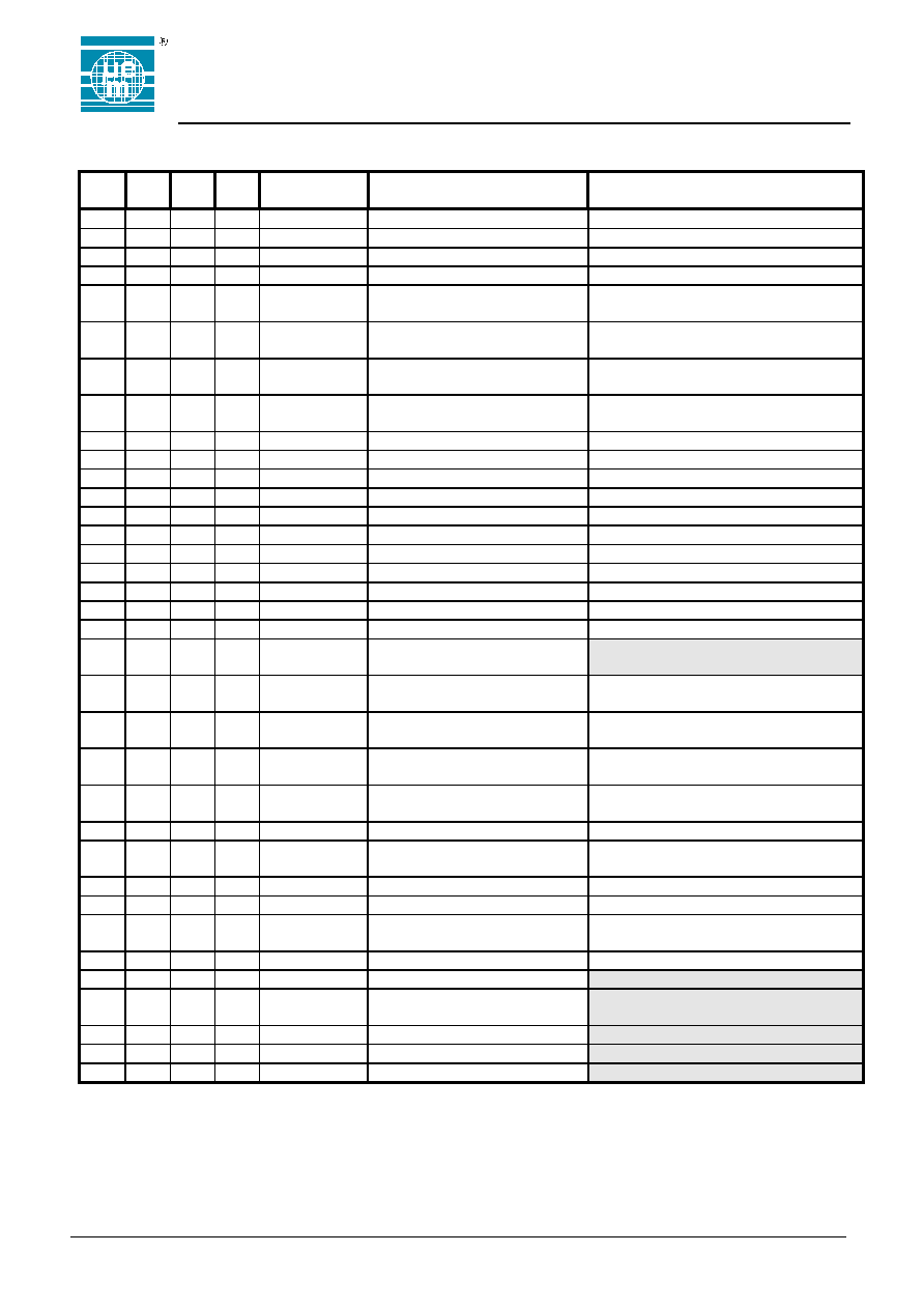
Figure 1. Architecture
Figure 2. Pin Configuration
EM MICROELECTRONIC
- MARIN SA

EM6520
03/02 REV. D/449
Copyright
2002, EM Microelectronic-Marin SA
2
www.emmicroelectronic.com
EM6520 at a glance
�
Power Supply
- Low voltage low power architecture
including internal voltage regulator
- 2.0 ... 5.5 V battery voltage
- 8 �A in active mode (Xtal, LCD on, 25
�C)
- 1.1 �A in standby mode (Xtal, LCD off, 25
�C)
- 0.1 �A in sleep mode (25
�C)
- 32 KHz Oscillator
� RAM
- 64 x 4 bit, direct addressable
� EEPROM
- 2048 x 16 bits programmable with EM's
standard MFP programming box
� CPU
- 4 bit RISC architecture
- 2 clock cycles per instruction
- 72 basic instructions
�
Main Operating Modes and Resets
- Active Mode (CPU is running)
- Standby Mode (CPU in halt)
- Sleep Mode (no clock, reset state)
- Initial reset on power on (POR)
- Watchdog reset (logic and oscillation watchdogs)
- Reset with input combination on port A (register
selectable)
�
Liquid Crystal Display Driver (LCD)
- 8 segments 3 or 4 times multiplexed
- Internal or external voltage multiplier
- Free segment allocation architecture
(metal 2 mask)
- LCD switch off for power save
�
4-Bit Input Port A
- Direct input read on the port terminals
- Debouncer function available on all inputs
- Interrupt request on positive or negative edge
- Pull resistor selectable by register
- Test variables (software) for conditional jumps
- PA[0] and PA[3] are inputs for the event counter
- PA[3] is Start/Stop input for the millisecond
counter
- Reset with input combination (register selectable)
�
Prescaler
- 15 stage system clock divider down to 1Hz
- 3 Interrupt requests; 1Hz, 32Hz or 8Hz, Blink
- Prescaler reset (4kHz to 1Hz)
�
4-Bit Bi-directional Port B
-
All different functions bit-wise selectable
- Direct input read on the port terminals
- Data output latches
- CMOS or Nch. open drain outputs
- Pull-down or pull-up selectable
- Pull-up in Nch. open drain mode
- Selectable PWM, 32kHz, 1kHz and 1Hz output
- Dynamic Input Comparator on PB[0] (SVLD level)
�
Voltage Level Detector
- Default value 2.4V
- Busy flag during measure
- Interrupt request at end of measure
�
10-Bit Universal Counter
- 10, 8, 6 or 4 bit up/down counting
- Parallel load
- Event counting (PA[0] or PA[3])
- 8 different input clocks-
- Full 10 bit or limited (8, 6, 4 bit) compare function
- 2 interrupt requests (on compare and on 0)
- Hi-frequency input on PA[3] and PA[0]
- Pulse width modulation (PWM) output
�
Millisecond Counter
- 3 digits binary coded decimal counter (12 bits)
- PA[3] signal pulse width and period measurement
- Internal 1000 Hz clock generation
- Hardware or software controlled start stop mode
- Interrupt request on either 1/10 Sec or 1Sec
�
Interrupt Controller
- 5 external and 7 internal interrupt request sources
- Each interrupt request individually maskable
- Each interrupt flag individually resettable
- Automatic reset of each interrupt request register
after read
- General interrupt request to CPU can be disabled
- Automatic enabling of general interrupt request
flag when going into HALT mode

EM6520
03/02 REV. D/449
Copyright
2002, EM Microelectronic-Marin SA
3
www.emmicroelectronic.com
Table of Contents
Features
1
Description
1
Typical Applications
1
EM6520 at a glance
2
1
Pin Description for EM6520
4
1.1
Programming Connections
5
2
Operating modes
6
2.1
ACTIVE Mode
6
2.2
STANDBY Mode
6
2.3
SLEEP Mode
6
3
Power Supply
7
4
Reset
8
4.1
Oscillation Detection Circuit
9
4.2
Input Port A Reset
9
4.3
Digital Watchdog Timer Reset
10
4.4
CPU State after Reset
10
5
Oscillator and Prescaler
11
5.1
Oscillator
11
5.2
Prescaler
11
6
Input and Output ports
13
6.1
Ports overview
13
6.2
Port A
14
6.2.1
IRQ on Port A
14
6.2.2
Pull-up/down
15
6.2.3
Software test variables
15
6.2.4
Port A for 10-Bit Counter and MSC
15
6.3
Port A registers
15
6.4
Port B
17
6.4.1
Input / Output Mode
17
6.4.2
Pull-up/Down
18
6.4.3
CMOS / NCH. Open Drain Output
18
6.4.4
PWM and Frequency output
19
6.5
PB[0] Dynamic Input Comparator
19
6.6
Port B registers
20
7
10-bit Counter
21
7.1
Full and Limited Bit Counting
21
7.2
Frequency Select and Up/Down Counting
22
7.3
Event Counting
23
7.4
Compare Function
23
7.5
Pulse Width Modulation (PWM)
23
7.5.1
How the PWM Generator works.
24
7.5.2
PWM Characteristics
24
7.6
Counter Setup
25
7.7
10-bit Counter Registers
25
8
Millisecond Counter
27
8.1
PA[3] Input for MSC
27
8.2
IRQ from MSC
27
8.3
MSC-Modes
28
8.4
Mode selection
28
8.5
Millisecond Counter Registers
30
9
Interrupt Controller
31
9.1
Interrupt control registers
32
10
Supply Voltage Level Detector
33
10.1
SVLD Register
33
11
RAM
34
12
LCD Driver
35
12.1
LCD Control
36
12.2
LCD addressing
36
12.3
Free segment allocation
37
12.4
LCD Registers
37
13
PERIPHERAL MEMORY MAP
39
14
Option Register Memory Map
42
15
Active Supply Current test
43
16
Mask Options
44
16.1
Input / Output Ports
44
16.1.1
Port A Metal Options
44
16.1.2
Port B Metal Options
45
16.1.3
Voltage Regulator Option
46
16.1.4
SVLD and Input Comp Level Option
46
16.1.5
Debouncer frequency Option
46
16.1.6
User defined LCD Segment allocation
46
17
Measured Electrical Behaviors
47
17.1
IDD Current
47
17.2
Regulator Voltage
47
17.3
Pull Resistors
47
17.4
Output currents
48
18
EM6520 Electrical specifications
49
18.1
Absolute maximum ratings
49
18.2
Handling Procedures
49
18.3
Standard Operating Conditions
49
18.4
DC characteristics - Power Supply
49
18.5
SVLD and Input Comparator
50
18.6
Oscillator
50
18.7
DC characteristics - I/O Pins
51
18.8
LCD Seg[8:1] Outputs
52
18.9
LCD Com[4:1] Outputs
52
18.10
DC Output Component
52
18.11
LCD voltage multiplier
52
19
Pad Location Diagram
53
20
Package & Ordering Information
54
20.1
Ordering Information
54
EM Microelectronic-Marin SA cannot assume responsibility for use of any circuitry described other than
circuitry entirely embodied in an EM Microelectronic-Marin SA product. EM Microelectronic-Marin SA reserves
the right to change the circuitry and specifications without notice at any time. You are strongly urged to ensure
that the information given has not been superseded by a more up-to-date version.
EM6520
03/02 REV. D/449
Copyright
2002, EM Microelectronic-Marin SA
4
www.emmicroelectronic.com
1 Pin Description for EM6520
Chip
QFP
44
DIL
40
QFP
32
Signal Name
Function
Remarks
1
13
7
9
C2B
Voltage multiplier
Not needed if ext. supply
2
14
8
10
C2A
Voltage multiplier
Not needed if ext. supply
3
15
9
11
C1B
Voltage multiplier
Not needed if ext. supply
4
16
10
12
C1A
Voltage multiplier
Not needed if ext. supply
5
18
11
13
VL1
Voltage multiplier level 1
LCD level 1 input, if external supply
selected
6
19
12
14
VL2
Voltage multiplier level 2
LCD level 2 input, if external supply
selected
7
20
13
15
VL3
Voltage multiplier level 3
LCD level 3 input, if external supply
selected
8
21
14
16
COM[4]
LCD back plane 4
Not used if 3 times multiplex
selected
9
25
17
17
COM[3]
LCD back plane 3
10
26
18
18
COM[2]
LCD back plane 2
11
27
19
19
COM[1]
LCD back plane 1
12
28
20
nc
SEG[8]
LCD segment 8
Not bonded for QFP 32
13
29
21
20
SEG[7]
LCD segment 7
14
30
22
21
SEG[6]
LCD segment 6
15
31
23
22
SEG[5]
LCD segment 5
16
32
24
23
SEG[4]
LCD segment 4
17
33
25
24
SEG[3]
LCD segment 3
18
35
27
25
SEG[2]
LCD segment 2
19
36
28
26
SEG[1]
LCD segment 1
20
37
29
27
Test
Input test terminal
Internal pull-down 15k
For EM tests only, GND 0 ! except
when needed for MFP programming
21
38
30
28
PB[0]
Input/output, open drain
port B terminal 0
Port B data[0] I/O or
dynamic input comparator input
22
39
31
29
PB[1]
Input/output, open drain
port B terminal 1
Port B data[1] I/O or
ck[12] output
23
40
32
30
PB[2]
Input/output, open drain
port B terminal 2
Port B data[2] I/O or
ck[1] output
24
41
33
31
PB[3]
Input/output, open drain
port B terminal 3
Port B data[3] I/O or
PWM output
25
43
35
32
PA[0]
Input port A terminal 0
Testvar 1
Event counter
26
1
36
1
PA[1]
Input port A terminal 1
Testvar 2
27
2
37
2
PA[2]
Input port A terminal 2
Testvar 3
28
3
38
3
PA[3]
Input port A terminal 3
Event counter
MSC start/stop control
29
5
39
4
VBAT=VDD
Positive power supply
MFP Connection
30
6
40
5
Vreg
Internal voltage regulator
Connect to minimum 100nF,
MFP Connection
31
8
1
6
Qout / Osc2
Crystal terminal
32kHz crystal, MFP Connection
32
10
3
7
Qin / Osc1
Crystal terminal
32kHz crystal, MFP Connection
33
11
5
8
VSS
Negative power supply
Reference terminal, MFP Connection
Gray shaded areas: terminals needed for MFP programming connections (VDD, VregLogic, Qin, Qout, Test, VSS). See
also Programming Connections.
EM6520
03/02 REV. D/449
Copyright
2002, EM Microelectronic-Marin SA
5
www.emmicroelectronic.com
Figure 3. Typical configuration
crysta l
LC D D isp lay
C 2
C 2
C 1
C 1
C 1
C 4
C 3
V reg
V S S
T est
V D D (V B A T )
S E G [8 :1]
Q IN Q O U T
C 1 A
C 1 B
C 2 A
C 2 B
C O M [4 :1 ]
V L 1
V L 2
V L 3
P o rt A
P o rt B
E M 6 5 2 0
all C apacitors 100nF
1.1 Programming
Connections
The EM6520 can be programmed using the standard EM MFP programming box for 4 bit uControllers. The
interface signals are listed in the table below. The circuit can be programmed on the programming box or
directly on the PCB . For more information please refer to the MFP programmer's manual.
Chip
QFP
44
DIL
40
QFP
32
Signal Name
Function
Remarks
20
37
29
27
Test
Input test terminal
Internal pull-down 15k
Usually 1 in MFP mode, 0 resets the
MFP interface
29
5
39
4
VBAT=VDD
Positive power supply
MFP Power Connection
30
6
40
5
Vreg
Internal voltage regulator
MFP power Connection, adapts the
Oscillator voltage to VBAT
31
8
1
6
Qout / Osc2
Crystal terminal
MFP Serial Data Input / Output
32
10
3
7
Qin / Osc1
Crystal terminal
MFP serial Clock Input
33
11
5
8
VSS
Negative power supply
MFP Connection, Reference terminal